
© Fraunhofer IMS/Andi Werner Photography
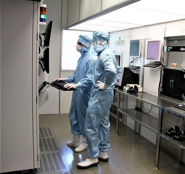
We support you in the development of novel and the improvement of existing circuit elements, that are used in modern applications, such as smart, connected sensor solutions.
Customised on-chip solutions for high-frequency applications
Precise analysis of new chips up to 120 GHz using spectral and network analysers; in-situ characterisation of bonded chips using network analysis up to 500 GHz
Validation of circuits under real conditions
Our portfolio includes post-CMOS technologies, MEMS, optical sensors and photonic circuits to give you a technological edge.
Utilisation of the latest semiconductor processes for higher integration densities and energy efficiency
Combination of mechanical and electrical components for compact systems
High-precision measurement solutions even under extreme environmental conditions
Integration of several functions on one chip to save costs and space
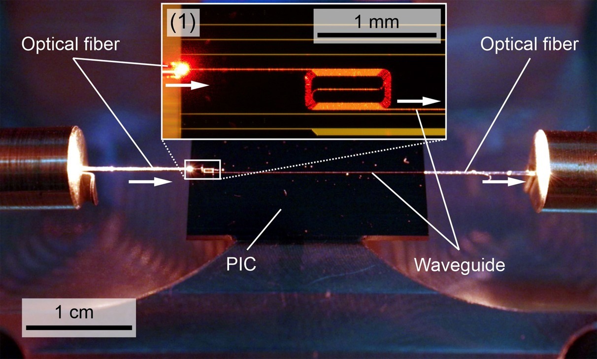
DSt: Co-Integration of optical and electrical functionalities on a single chip for cost- and size-reduction
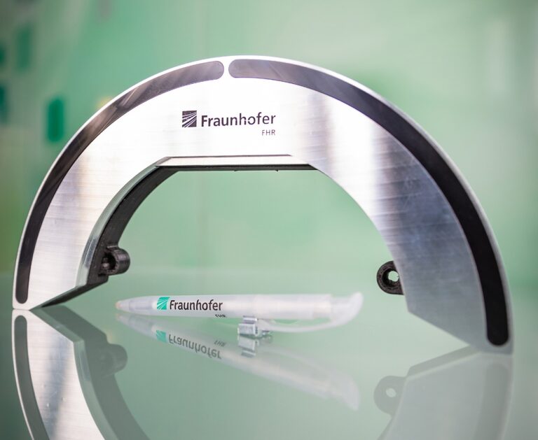
Material and module analysis for the terahertz range
© Fraunhofer IMS
© Fraunhofer IMS
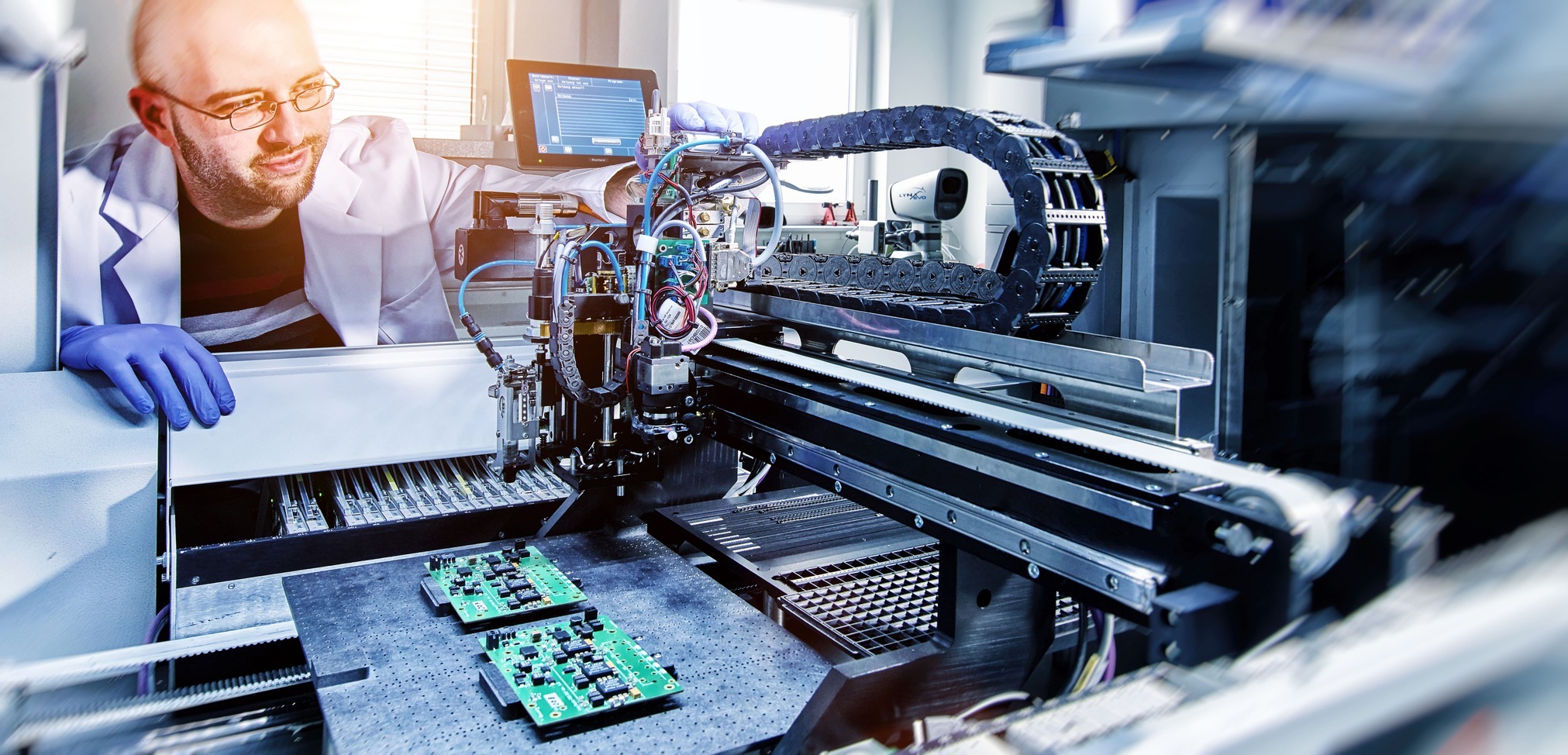
We transform your product vision into market-ready solutions – supported by rapid prototyping, 3D printing and in-house PCB assembly.
Rapid realisation with state-of-the-art prototyping techniques
From automated electronics assembly to CNC machining - for reproducible quality
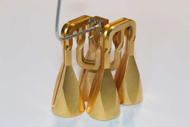
Complex wireless systems, antennas and filters up to 120 GHz
Our production centre guarantees maximum precision at every stage.
Wire bonding with materials such as gold and aluminium wires for RF-compatible connections of the highest precision (placement accuracy <5 µm) as well as chip-film patch for mechanically flexible systems by bonding on polyimide films and hybrid bonding by combining different chip technologies (CMOS + MEMS) in a single package.
Starting with fully automated assembly with automated optical inspection (AOI), we have the core competences of an electronics manufacturing serives (EMS) provider. Due to the in-house operation of our machinery, including internal material procurement, lead times for prototypes are drastically reduced, while maximising flexibility. For larger batches, we have a partner network of qualified EMS and use industry standards for exchange formats.
5-axis CNC machining for the production of precise high-frequency components (down to the lower terahertz range); use of 3D printing processes (including metal and plastic laser sintering) for millimetre-wave components; electroplating surface finishing (gold/nickel plating) even at sub-millimetre wavelengths.
© Fraunhofer FHR
© Fraunhofer IMS
Optical interfaces
Bonding of photonic chips with electronic circuits (e.g. for LiDAR systems)
QMI-Technology
Quantum dot midwave infrared integration for improved optical coupling
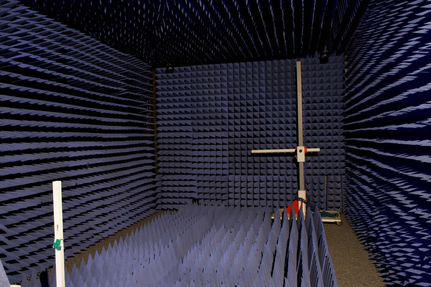
Our laboratories with an anechoic antenna measurement chamber enable interference-free analyses.
Spectral and network analysis
Up to 120 GHz
Time domain measurements
Multi-channel systems up to 65 GHz
Material characterisation
Non-destructive testing methods for quality management and research
© Fraunhofer IMS
© Fraunhofer FHR
Strengthen your technological edge – with a partner who combines terahertz expertise and industrial practice.
Scientific excellence: Access to the latest research results from the Fraunhofer Institutes.
One technology, many possible applications
Take advantage of our terahertz expertise and industrial experience for your technological advantage. Whether medical technology, security or communication – together we will realise your innovation.
Um Ihnen ein optimales Erlebnis zu bieten, verwenden wir Technologien wie Cookies, um Geräteinformationen zu speichern und/oder darauf zuzugreifen. Wenn Sie diesen Technologien zustimmen, können wir Daten wie das Surfverhalten oder eindeutige IDs auf dieser Website verarbeiten. Wenn Sie Ihre Zustimmung nicht erteilen oder zurückziehen, können bestimmte Merkmale und Funktionen beeinträchtigt werden.
Adding {{itemName}} to cart
Added {{itemName}} to cart