Low-noise, highly stable terahertz sources based on lasers, and highly sensitive detectors enabled by photodiodes – compactly integrated on silicon chips: photonic technologies are key enablers of terahertz sensing.
With our photonic development platform, we conduct research and develop high-performance, compact, and application-oriented terahertz systems within a research-driven framework.
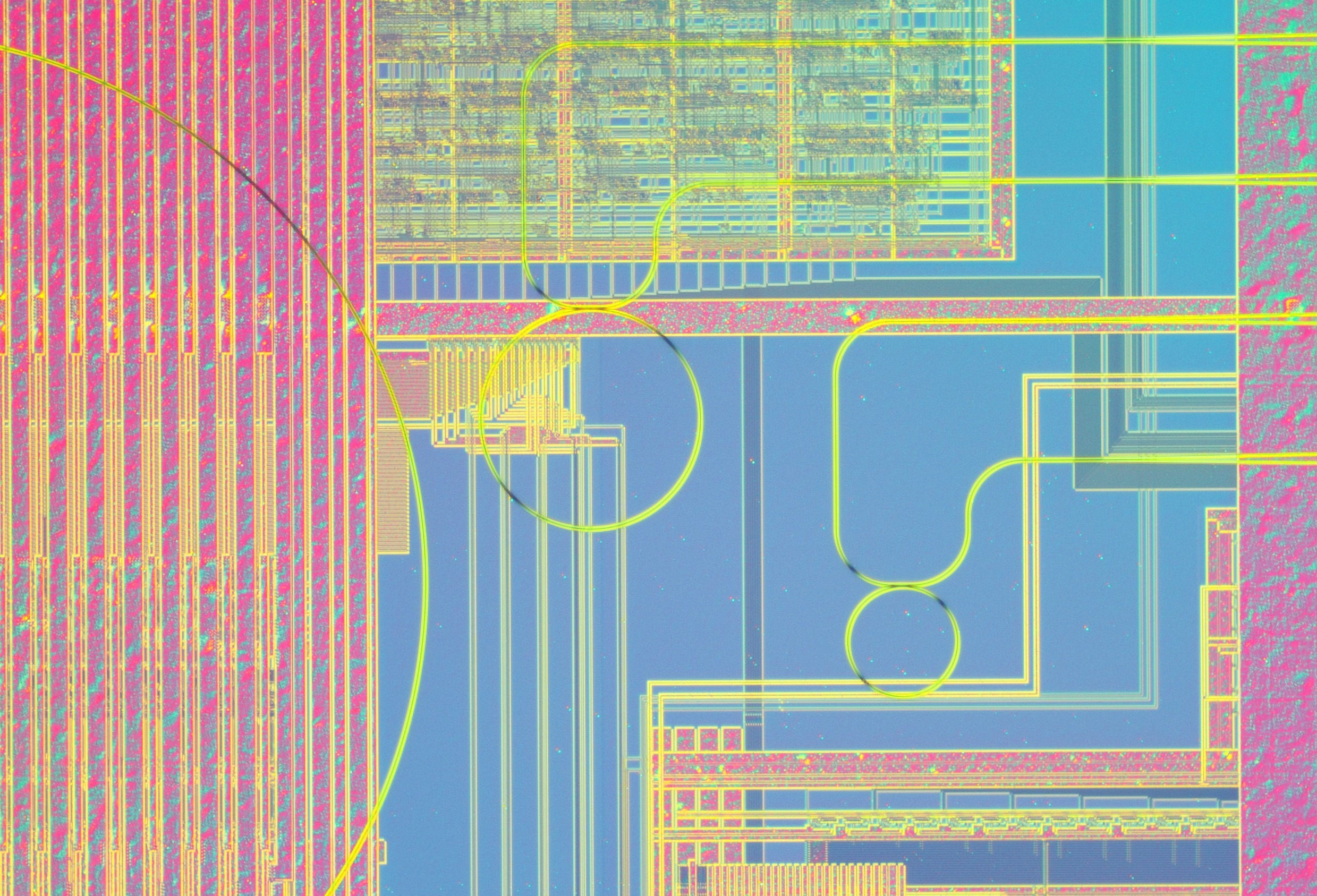
Photonics and electronics on a chip: Photonic ring resonators are arranged above the CMOS circuits. © Fraunhofer IMS
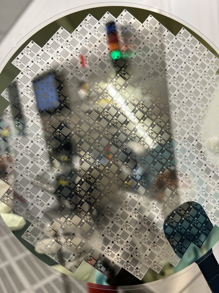
© Fraunhofer IMS
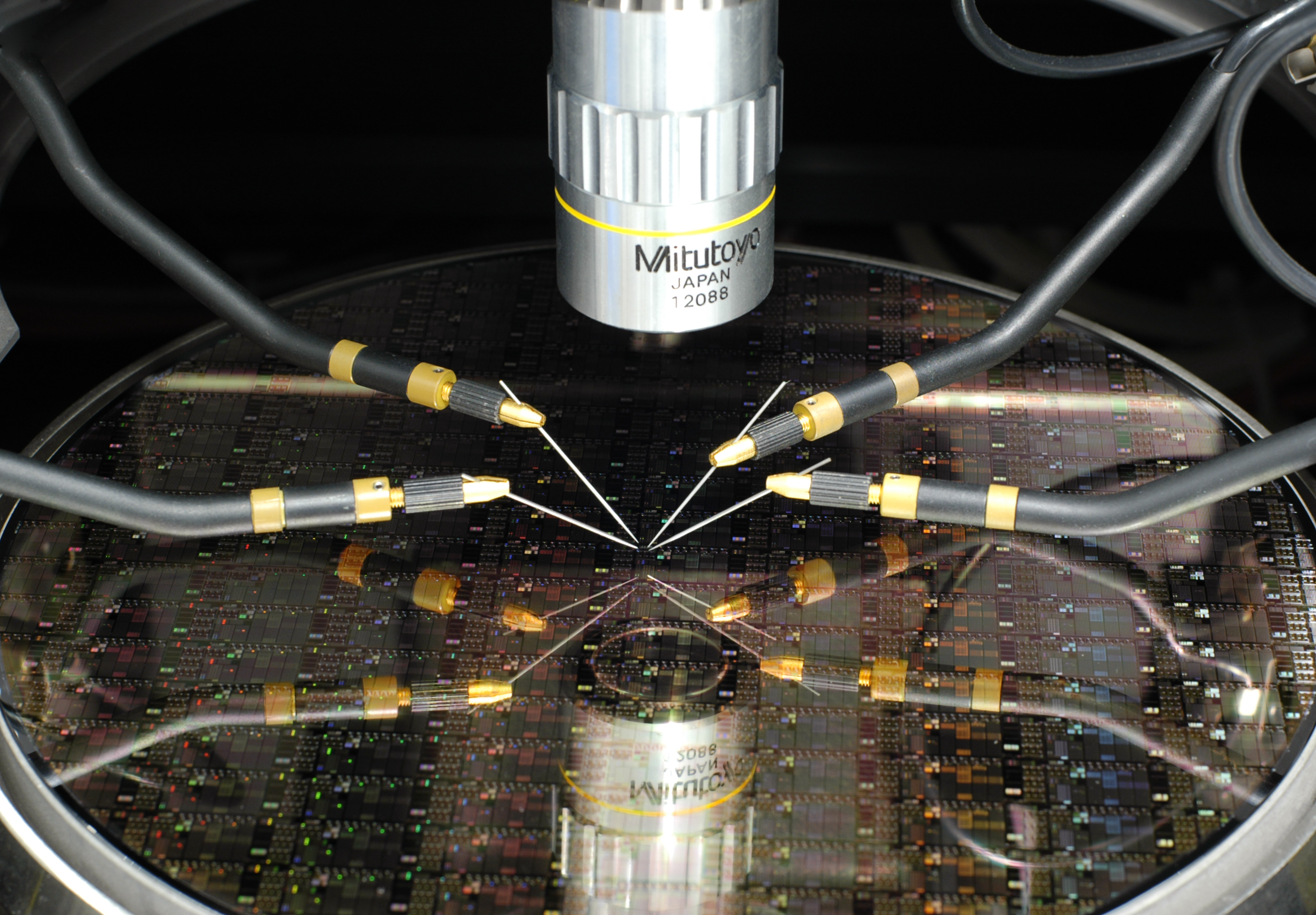
© Fraunhofer IMS
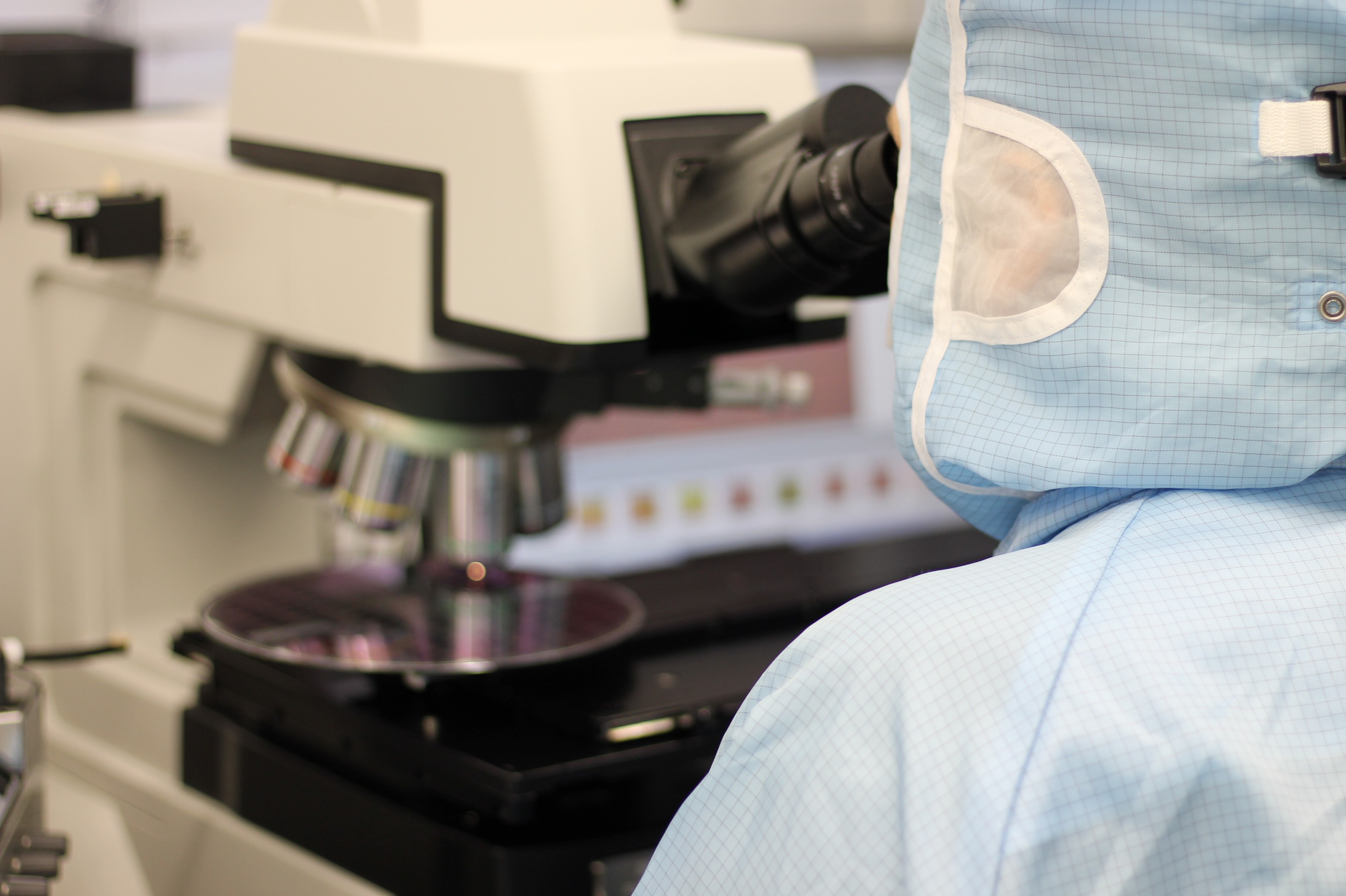
© Fraunhofer IMS
Our photonic platform enables solutions across a wide range of application areas:
Our sensor technologies combine the high signal quality of established CCD sensors (charged-coupled devices) with the flexibility and performance of modern CMOS circuitry. This advanced integration reduces parasitic effects and enables enhanced signal processing in demanding applications. High-purity, low-defect silicon is used as the base material to minimize dark current. Optimized gate structures and deep channel implantations promote low-loss charge transport and high transfer efficiency.
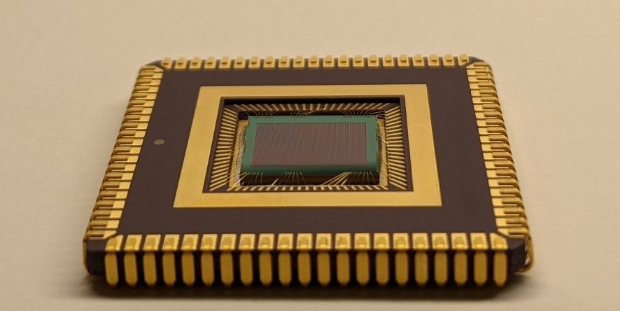
CSPAD image sensor. © Fraunhofer IMS
LiDAR (Light Detection and Ranging), with its precise three-dimensional acquisition of environments and objects, is a key technology for advanced driver assistance systems, autonomous vehicles, and industrial robotics. For highly sensitive 3D imaging, we integrate CSPAD technology (CMOS single-photon avalanche diodes) into LiDAR systems for effective background light suppression, high resolution and reliable distance measurements. By combining these approaches with Photonic Integrated Circuits (PICs), we further enhance range and functionality.
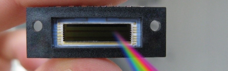
3D image sensor for flash LiDAR camera systems. © Fraunhofer IMS
Our platform creates valuable synergies for the development of high-performance, miniaturized sensor components that can be flexibly deployed in both the optical and terahertz domains while complying with CMOS standards. Through these innovations, we contribute to advancing technologies in areas such as security and environmental monitoring – benefiting society while meeting industrial requirements.
Adding {{itemName}} to cart
Added {{itemName}} to cart